Materials Foundries: Turning Lab Breakthroughs into Repeatable Supply
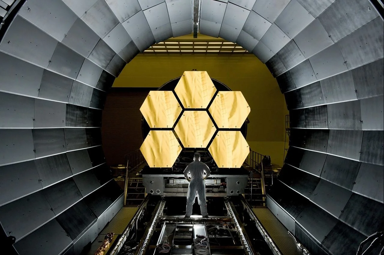
The James Webb Space Telescope incorporates carbon fibre composite, gold-coated beryllium, and graphite composite in its construction.
Credit: NASA/David Higginbotham
From one-off wonders to parts you can order twice
The James Webb Space Telescope is a monument to materials programmes done properly—carbon-fibre composites for stiffness, gold-coated beryllium for mirrors that hold shape at cryogenic temperatures, graphite composites where weight and stability fight for primacy. None of that arrived from a hype cycle. It arrived from foundry-grade discipline: process recipes, metrology, qualification, and suppliers who could make the same thing again and again.
That is the point of a materials foundry. It’s the bridge between a paper and a purchase order, where a promising film, fibre or powder becomes a repeatable product with tolerances, testing and a price. If you’re picturing a silicon fab, you’re not far off—just swap transistors for coatings, tapes and laminates. The work is the same: lock the process, measure everything, and prove that the tenth run behaves like the first.
The temptation, especially with 2D materials, is to spread the jam too thin: a dozen demo projects, none quite production-ready. Foundries force the opposite. They narrow the stack to what can be made at scale and yield, then publish the rules that designers can live with. Terms that sound like insider code are simply the grammar of reliability. Process recipes are step-by-step instructions—temperatures, gas flows, timings—that turn a lab step into a production step. Metrology is the toolkit that checks thickness, roughness, crystal quality and defects on every run. Statistical process control is the habit of plotting those measurements and stopping the line when drift appears. It’s dull, and it’s where value lives.
Why does it matter now? Because the bottleneck has moved from ideas to availability. Battery makers want silicon-rich anodes that don’t swell and crack. Aerospace primes want heat-resistant composites that don’t creep at 300 °C. Chipmakers want wide-bandgap materials—silicon carbide (SiC), gallium nitride (GaN)—to run power electronics cooler and smaller. Lab breakthroughs exist; what buyers lack is assured supply with data sheets you can put in a contract. That is a foundry’s product.
A useful mental model is to treat new materials like a platform, not a product. In semiconductors the PDK—process design kit—tells designers what they can draw and what they’ll get back. Materials need the equivalent: call it an MDK. It would define film thickness ranges, grain sizes, interface adhesion, lay-up rules, permitted dopants, joining methods, and environmental limits. It would include design controls (“no features sharper than X; minimum radius Y; stack in this order to avoid delamination”) and test coupons that customers can run in their own labs. Publish that, and you’ve turned a curiosity into a building block.
The business model follows naturally. Early revenue is qualification: paid runs that produce enough material for customers to test to their own standards, plus the reports to match—micrographs, X-ray diffractograms, peel tests, fatigue curves. Next comes offtake: multi-year agreements that trade price for volume and priority. Then co-development: you tweak the recipe to a customer’s device and lock it behind a change-control gate so nothing drifts without both sides signing. The finance community knows how to underwrite that. It’s the same logic that took carbon fibre from race cars to airliners, and beryllium from physics labs to space telescopes.
A word on scale, because it gets abused. “Wafer-scale” or “panel-scale” simply mean the area of each unit you can make consistently—200 mm wafers, metre-class panels, kilometre-class tapes. If your customer needs ten square metres of a coating for a satellite radiator and your best lot is a hand-span, you don’t have a product yet—you have a sample. Likewise, yield is not a vibe; it’s the percentage of area or reels that pass spec without rework. Until yield clears 80–90% on representative runs, plan for delays and scrap.
None of this precludes ambition. Graphene and other 2D materials will earn their way into structures and electronics; the question is sequencing. Follow Webb’s lesson: pick applications where the value is obvious and the stack is disciplined. A gold-coated beryllium mirror is not fashionable, but it held shape in the cold vastness of space because a supply chain backed it. A graphene barrier layer that halves moisture ingress in a battery pouch is not glamorous either—but if a foundry can make it at panel-scale with documented adhesion and lifetime, it’s a business.
Buyers should read materials pitches the way they read turbine or chip pitches—by the artefacts, not the adjectives. Ask for a process flow, not a slide. Ask what inline metrology catches drift and how many lots have run without operator intervention. Ask for the change-control plan: if a precursor supplier swaps formulation, how will you know, and who re-qualifies? Ask how the line handles contamination—what are the clean-down cycles, how are tools segregated, which solvents touch the product? These are not traps; they are the questions that keep schedules real.
The people question matters as much as the plant. A credible foundry blends three tribes: researchers who understand the physics of the material, production engineers who can make it behave on a Tuesday afternoon, and quality teams who can say “no” when a run looks pretty but falls outside control limits. Put them in one building with procurement that can source weird precursors and logistics that can ship hazardous cylinders without drama, and you have a business. Split them, and you have meetings.
There is, finally, the politics of localisation. Governments want strategic materials made at home; companies want to buy from whoever ships on time. The sane answer is staged: build the first qualified line where capability already exists; export the frozen process and training to a second site once yields are stable; and only then mandate domestic content. The result is resilience without pretending that skills can be magicked into being by decree.
So if the James Webb image looks out of place in a story that doesn’t mention graphene, it shouldn’t. It is a reminder that the materials that change industries are the ones that make it out of the lab and into a supply chain that never misses a Tuesday. A materials foundry is how you make that leap: less about “breakthroughs,” more about boring excellence—recipes that hold, measurements that catch drift, and contracts that turn repeatability into margin.
The prize is straightforward. When designers can rely on a new film, fibre or laminate the way they rely on a bolt or a bearing, innovation speeds up elsewhere: lighter buses, cooler inverters, quieter aircraft, better batteries. That’s how materials foundries pay for themselves—by making the extraordinary ordinary, and by letting the next Webb take shape without anyone asking whether the supplier can do it twice.